
Modbus TCP Acquisition
Description: Depending on the transmission medium, Modbus can communicate over serial ports or network ports (including fiber). RTU uses serial communication, while TCP uses network ports (Ethernet). The Modbus protocol follows a master/slave communication sequence. The edge gateway’s Modbus driver operates as a Master client [master device], actively sending queries to Modbus slave devices. Each slave prepares a response based on the received request and sends it back to the gateway.
1. Create nodes
Section titled “1. Create nodes”(1) Open Digital Twin in CommBridge, then select Device Connectivity on the left.
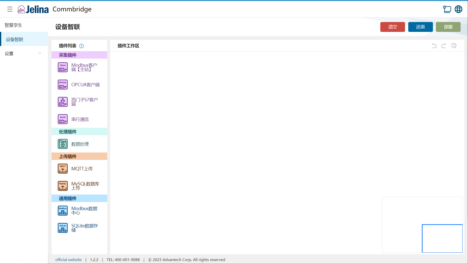
(2) Drag the Modbus Client [Master], Data Processing, and MQTT Upload plugins to the plugin workspace to create three nodes.

(3) Connect the three nodes in this order: Modbus Client [Master] → Data Processing → MQTT Upload.

2. Create a scheme
Section titled “2. Create a scheme”Select
Modbus-TCPas the protocol.
(1) Double-click Modbus Client [Master], then click Add Scheme.
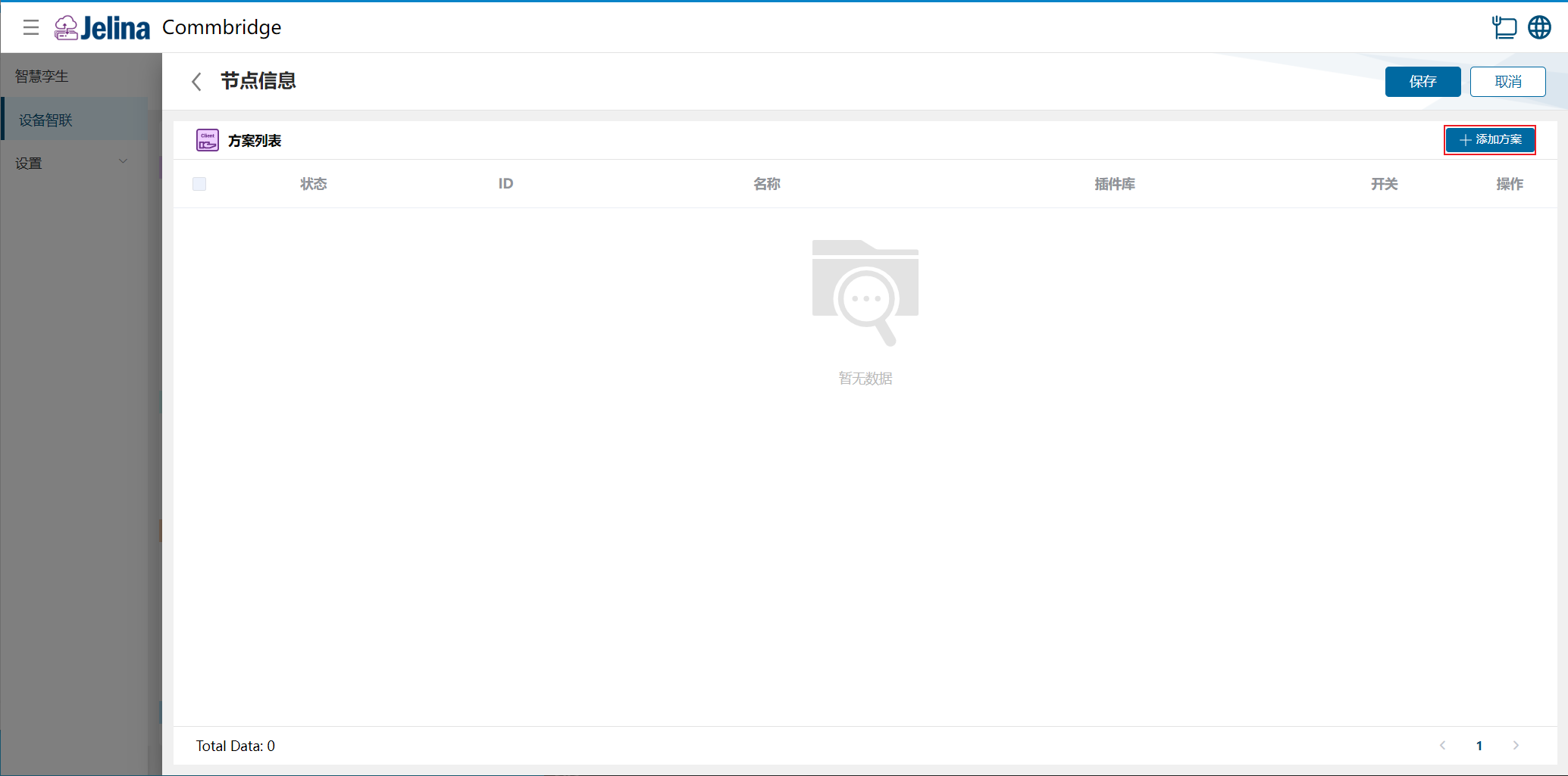
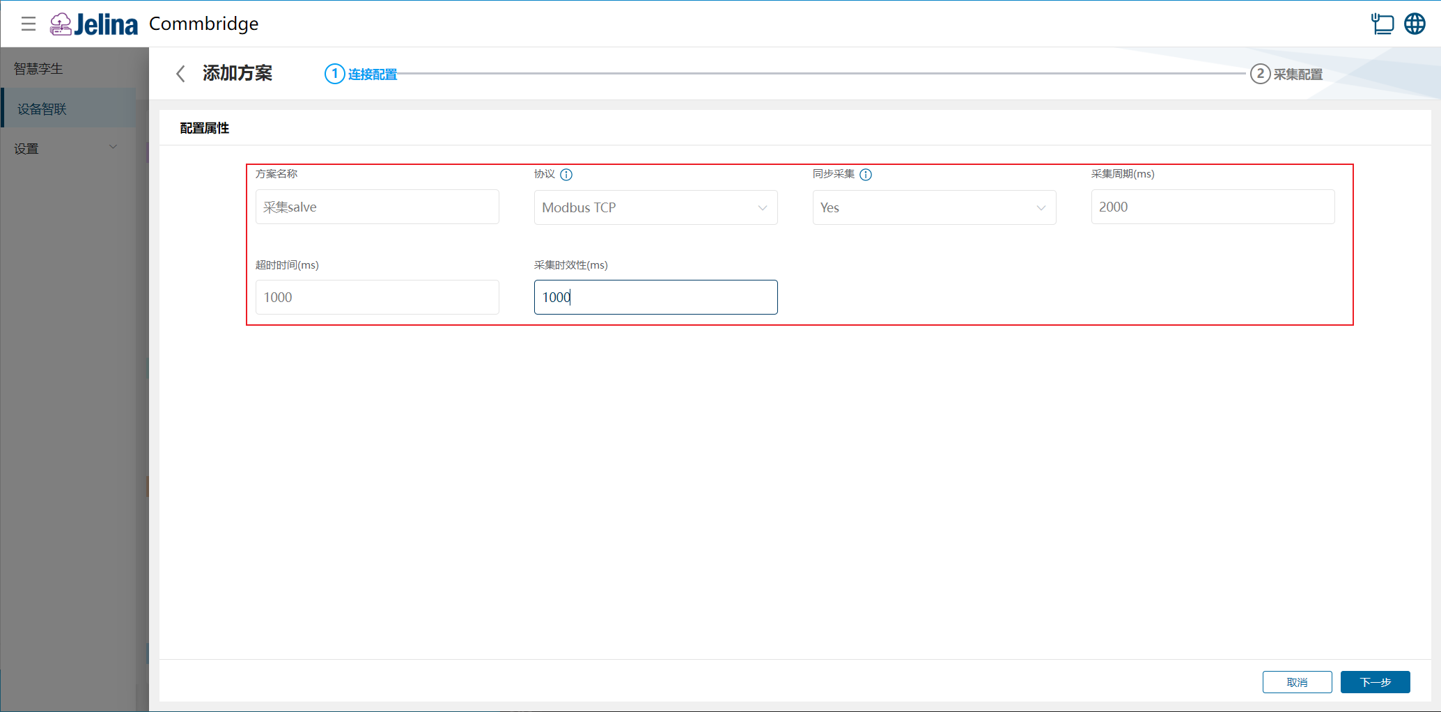
(2) Enter the connection settings, then click Next.
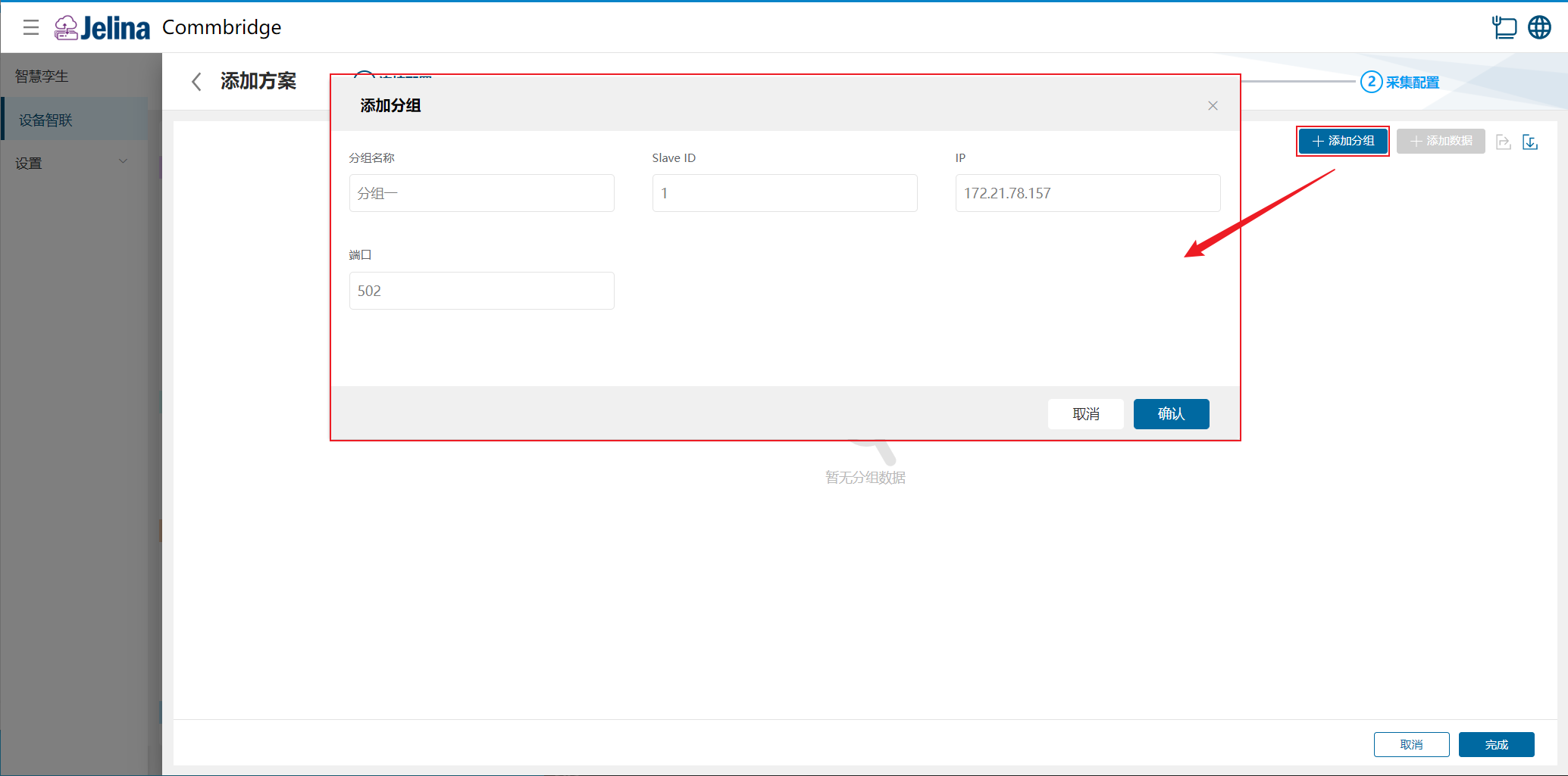
(3) Click Add Group, enter the group settings, then click Confirm.
(4) Click Add Data, enter the point settings, then click Confirm.
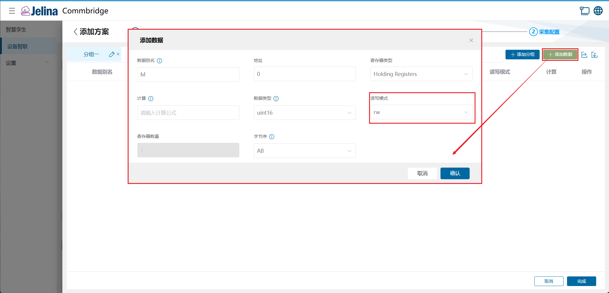
(5) Click Finish to add the acquisition scheme.
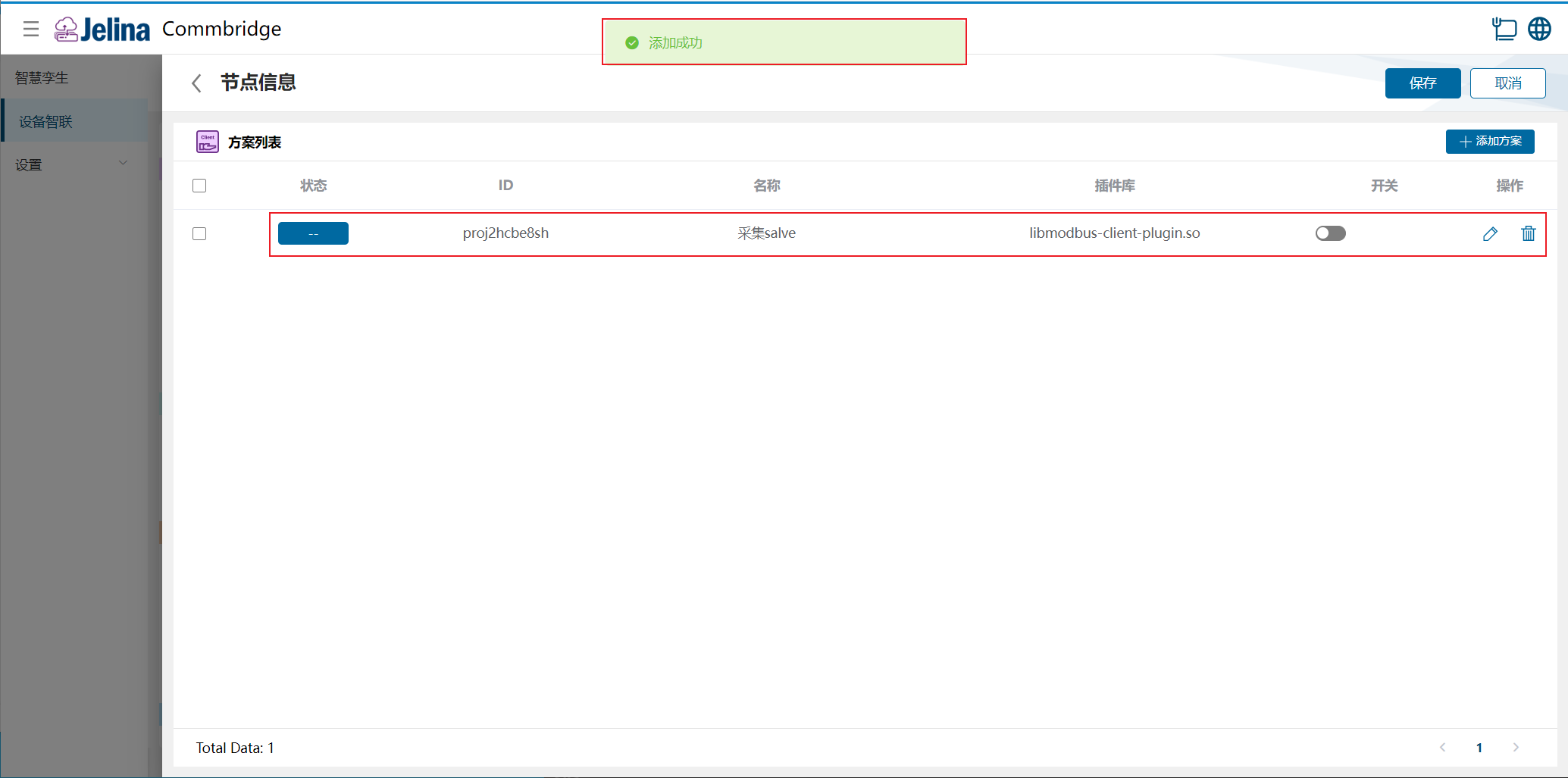
(6) Enable the scheme, then click Save.
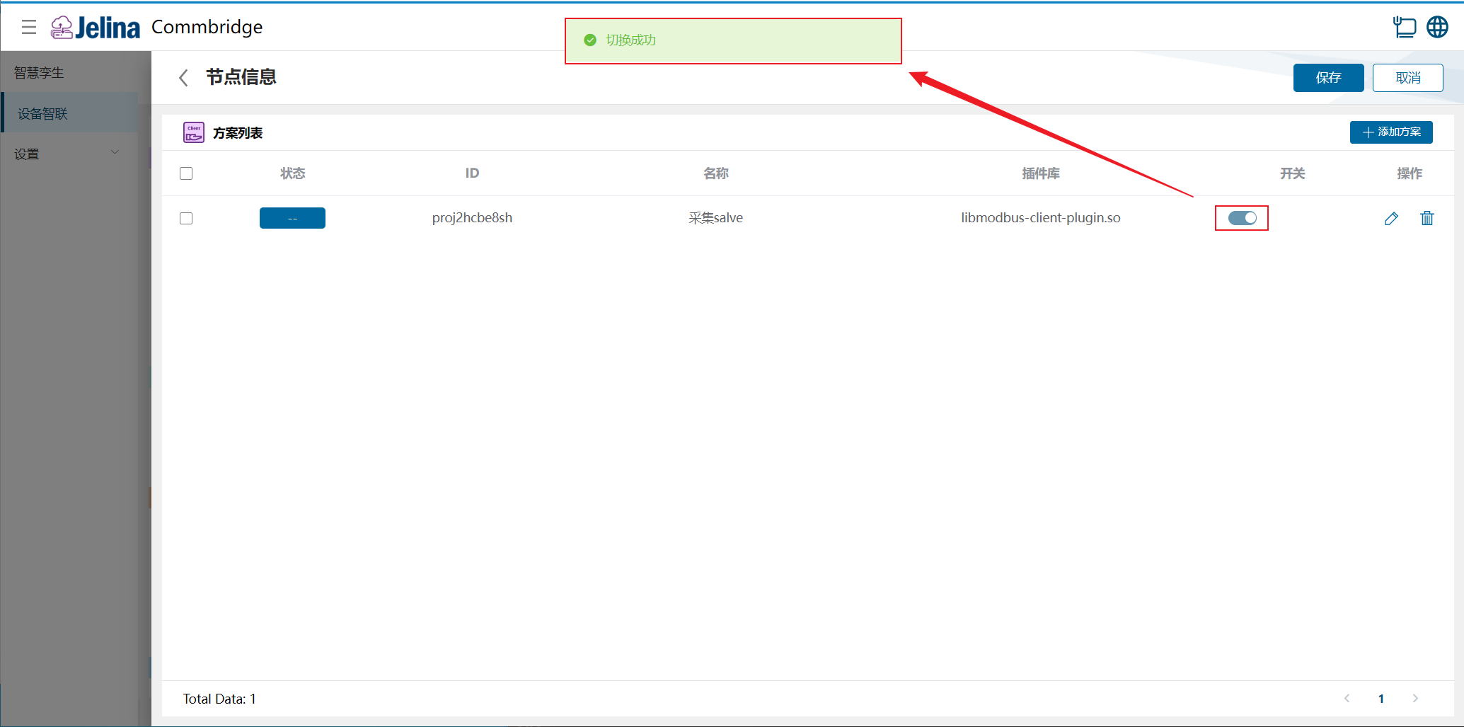
3. View results
Section titled “3. View results”(1) Click Deploy in Device Connectivity to deploy successfully.
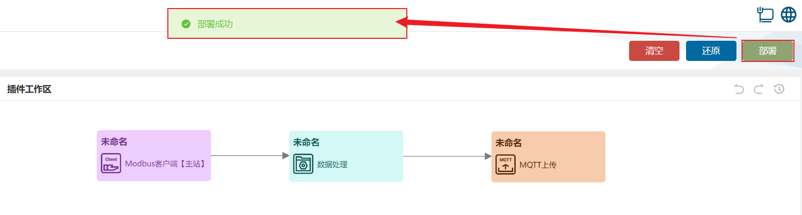
(2) Switch to Digital Twin and hover over the Modbus Client [Master] node to display its information list.
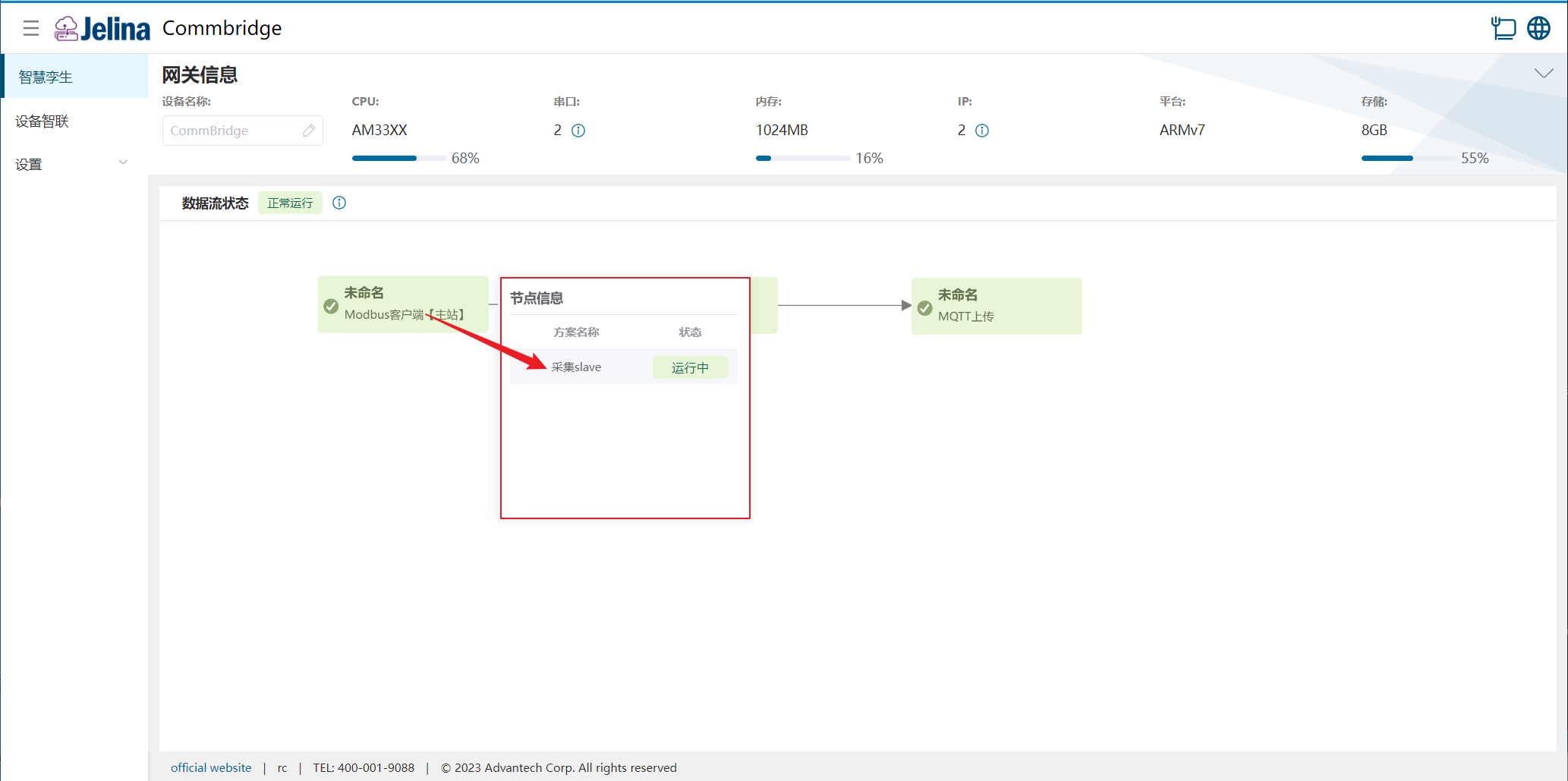
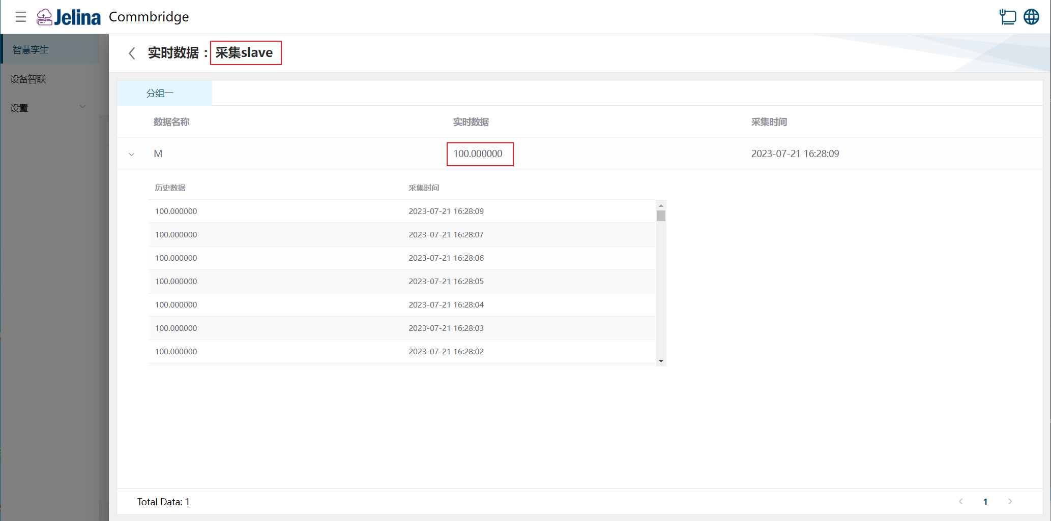
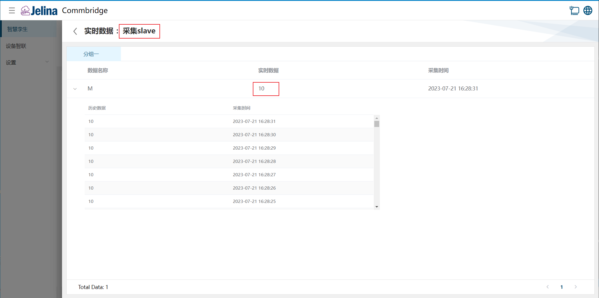
(3) Click the scheme to view real-time and historical point data for its groups.
Acquired data (before processing):
After processing (view the scheme in the Data Processing plugin):
4. Write data
Section titled “4. Write data”Data can only be modified when the point’s read/write mode is
rworwoand acquisition is operating normally.
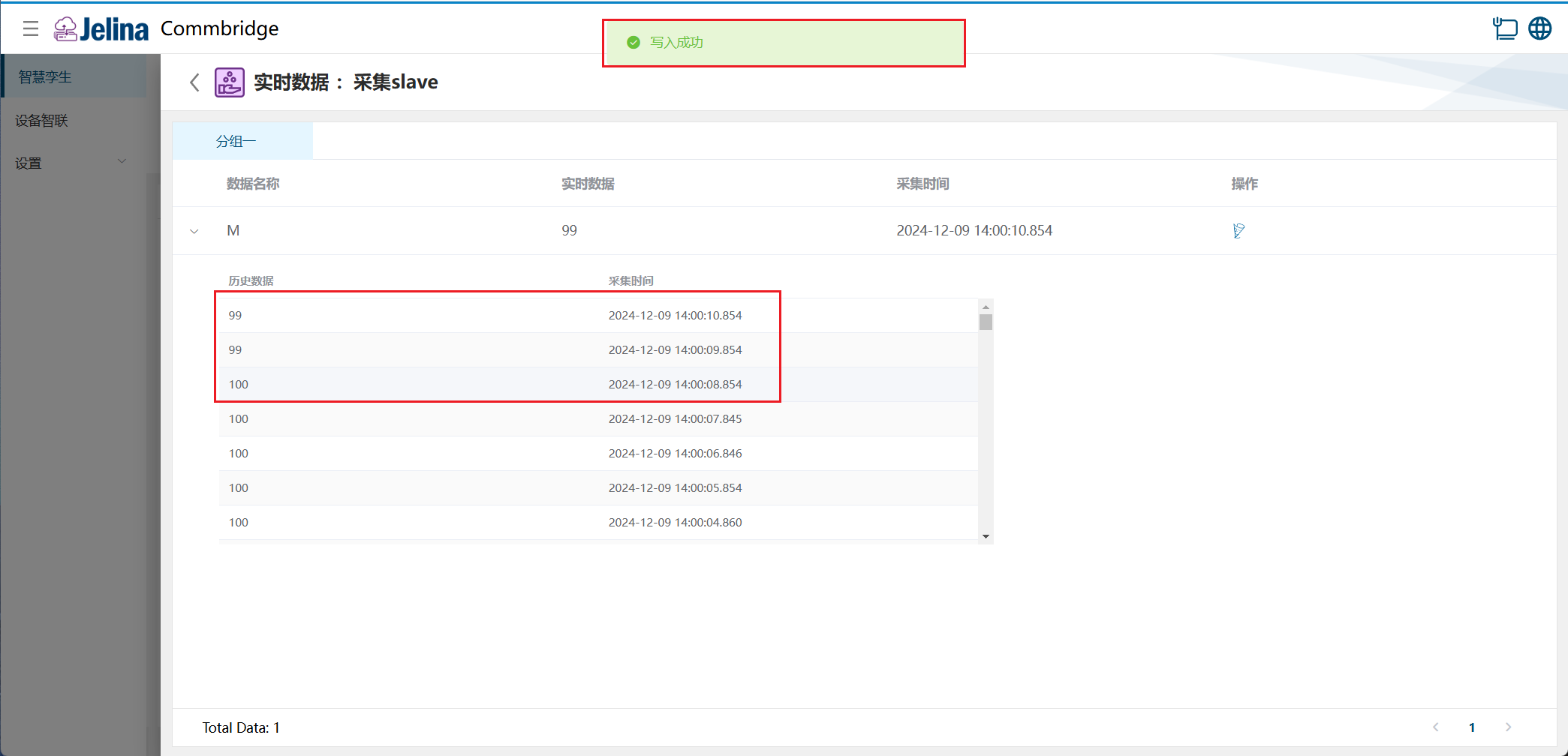
(1) Click Write for a data item, configure its data, then click OK.
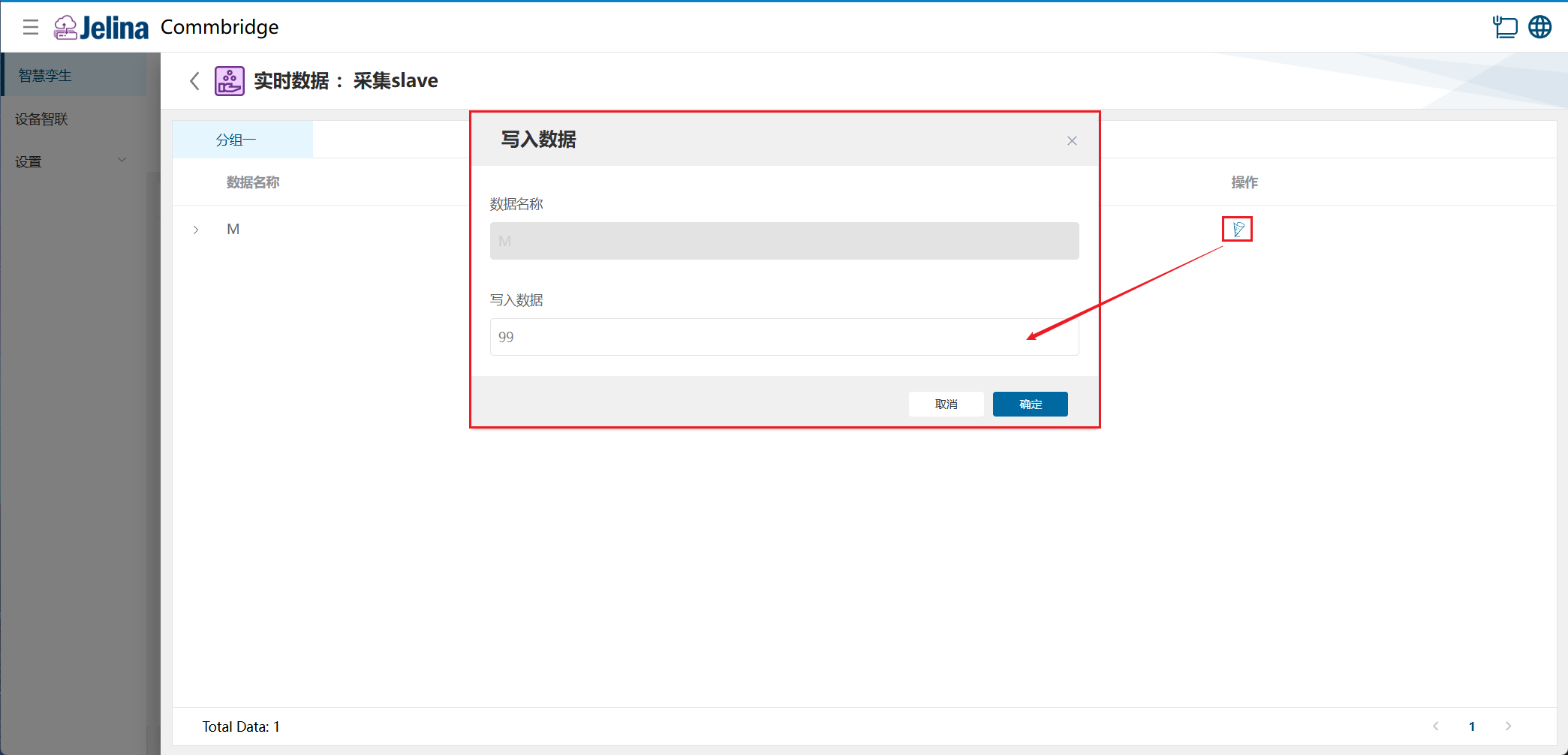
(2) View historical data.
5. Configuration details
Section titled “5. Configuration details”Connection settings
Section titled “Connection settings”| Parameter | Description | Format | Example |
|---|---|---|---|
| Scheme name | User-defined name for the scheme | Nonempty | Slave acquisition |
| Protocol | Modbus protocol | Modbus TCP, Modbus RTU | Modbus TCP |
| Synchronous acquisition | Whether to use synchronous acquisition: Yes or No | Yes, No | YES |
| Acquisition interval | Polling interval for reading data: the interval between register reads for each group in the scheme | Number, range: (100,2147483647] | 2000 |
| Acquisition freshness | All points in a group must be acquired within this period, including frame delays; otherwise the group’s data is discarded | Number, range: (0, acquisition interval] | 1000 |
| Timeout | Maximum duration of each acquisition for each group in the scheme; data from a read is discarded if this time is exceeded | Number, range: (0, acquisition interval] | 1000 |
| Maximum batch register count | Maximum number of registers per batch when acquiring consecutive points | Natural number, range: [1,120] | 120 |
| Frame delay | Minimum interval between acquisitions; the default is 0. Increase it if acquisition frequently times out; otherwise leave it unchanged | Milliseconds; number, range: [0, 2147483647] | 0 |
| Write frame delay | Additional wait when writing data, required by some devices with slow write operations; 0 means no extra delay | Milliseconds; number, range: [0, 2147483647] | 0 |
| Write register function code | Function code for writing holding registers | Auto, 06, 10; see below | Auto |
| Change-based acquisition | Acquisition mode. No: no change-based filtering; SingleData: transmit only points that change; WholeGroup: transmit the entire group when any data in the group changes | No, SingleData, WholeGroup | SingleData |
| Change-based acquisition reset time | Forces a data submission when data remains unchanged for longer than this period. Set to 0 to never trigger it | Seconds; number, range: (0, 2147483647] | 0 |
| Failure backoff | Extends the time before the next acquisition according to the backoff factor after a failure, up to acquisition interval × maximum backoff factor | Yes, No; see below | Yes |
| Backoff factor | Time multiplier on failure; must be greater than 0 and not equal to 1 | Number | 2 |
| Maximum backoff factor | Maximum time multiplier; once reached, this multiplier remains unchanged | Number | 16 |
Synchronous acquisition:
- “Yes” uses a common acquisition interval, timeout, and acquisition freshness setting for all groups in the scheme. These settings apply to all point data in the scheme.
- “No” allows each group to configure its own acquisition interval, timeout, and acquisition freshness.
Write register function code: Auto uses 06 when writing one register and 10 when writing more than one register; 06 uses 06 for all register writes; 10 uses 10 for all register writes.
Failure backoff: for an acquisition interval of 1 second, a backoff factor of 2, and a maximum backoff factor of 16, successive acquisition failures produce waits of 1s, 2s, 4s, 8s, and 16s. Similarly, for an acquisition interval of 10 seconds, a backoff factor of 0.5, and a maximum backoff factor of 0.1, successive failures produce waits of 10s, 5s, 2.5s, and 1.25s. A successful acquisition restores the initial default acquisition interval.
When the backoff factor is greater than 1, the maximum backoff factor must be greater than the backoff factor. When it is less than 1, the maximum backoff factor must be less than the backoff factor.
Add a group
Section titled “Add a group”| Parameter | Description | Format | Example |
|---|---|---|---|
| Group name | User-defined name for the group | Nonempty | Group 1 |
| Slave ID | Modbus device address: the slave address of the device being polled | Number, range: (0,255] | 1 |
| IP | IP address of the Modbus device | Address in dotted-decimal notation | 172.21.78.157 |
| Port | Port number of the Modbus device; defaults to 502 | Number, range: (0,65535] | 502 |
| Acquisition interval | Data polling interval: the interval between register reads for this group | Number, range: (100,2147483647] | 2000 |
| Acquisition freshness | Validity window for acquiring all points in this group. If all point data is not read within this period, all point data in the group is discarded | Number, range: (0, acquisition interval] | 1000 |
| Timeout | Maximum duration of each acquisition for this group; data from the read is discarded if this time is exceeded | Number, range: (0, acquisition interval] | 1000 |
Note: When Synchronous acquisition in the connection settings is No, these settings apply to all point data in the group. Modbus limits the number of registers that can be read at once. A single read supports at most 120 consecutive Holding Register or Input Register points, or 2000 consecutive Discrete or Coils points.
Add data
Section titled “Add data”| Parameter | Prerequisite | Description | Format | Example |
|---|---|---|---|---|
| Data alias | Point name, unique within the group | Nonempty; cannot start with a digit or underscore, or contain spaces | M | |
| Address | Register address, unique within the group | Register address, unique within the group | Number, range: (0,2147483647) | 0 |
| Register type | Modbus operation code | Holding Register, Input Register, Discrete, Coils; see below | Holding Register | |
| Data type | Determined by the register type | Raw data type of the register | uint16, int16, uint32, int32, float, boolean, combine, string, hex string; see below | uint16 |
| Byte order | Determined by the register type and data type | Storage order in memory for data types larger than one byte | AB, BA, ABCD, CDAB, BADC, DCBA; see below | AB |
| Register count | Determined by the register type and data type | Number of registers occupied by the data type | See below | 1 |
| Read/write mode | Determined by the register type | Supports ro (read only), rw (read/write), and wo (write only) | ro, rw, wo | ro |
| Calculation | User-defined formula based on the data alias | {M}/10 | ||
| Offset | Data type is bit | Bit offset from high to low after byte-order adjustment | Number, range: [0,15] |
For example, if the temperature property on your device is at address 1, set the register address to 1 when testing that property.
- For Discrete and Coils registers, the data type defaults to boolean.
- For uint16, int16, and combine, the available byte orders are AB and BA. For uint32, int32, and float, they are ABCD, CDAB, BADC, and DCBA. Other data types have no byte-order setting.
- For Discrete and Coils, the register count defaults to 1. For uint16, int16, and boolean, it defaults to 1. For uint32, int32, and float, it defaults to 2. For combine, select 1 or 2. For string and hex string, enter the register count manually.
16-bit order:
- AB: a one-word register, with the high word before the low word and the high byte before the low byte within the word (big-endian).
- BA: a one-word register, with the high word before the low word and the low byte before the high byte within the word (little-endian).
32-bit order:
- ABCD: two words, with the high word before the low word and the high byte before the low byte within each word (big-endian).
- BADC: two words, with the high word before the low word and the low byte before the high byte within each word (big-endian with byte swap).
- CDAB: two words, with the low word before the high word and the high byte before the low byte within each word (little-endian with byte swap).
- DCBA: two words, with the low word before the high word and the low byte before the high byte within each word (little-endian).
6. Modbus protocol parameter details
Section titled “6. Modbus protocol parameter details”The register type determines the data type, register count, and read/write mode.
Register types
Section titled “Register types”0x, 1x, 3x, and 4x are address ranges defined by the Modbus protocol.
| Register type | Name | PLC register address | Protocol register address | Read/write access | Description |
|---|---|---|---|---|---|
| Holding Register | Holding register (4x) | 40001-49999 | 0000H-FFFFH | Read/write; read: 0x03, write: 0x06 | Output or stored parameters: parameters configured while the controller is running |
| Input Register | Input register (3x) | 30001-39999 | 0000H-FFFFH | Read only, 0x04 | Input parameters obtained from external devices while the controller is running |
| Discrete | Discrete input status (1x) | 10001-19999 | 0000H-FFFFH | Read only, 0x02 | Input ports whose states are changed by external settings |
| Coils | Coil status (0x) | 00001-09999 | 0000H-FFFFH | Read/write; read: 0x01, write single coil: 0x05, write multiple coils: 0x0F | Output ports whose output states can be set and read |
Data types
Section titled “Data types”The data type is determined by the raw data type, whether the high and low bytes within registers are swapped, and whether the register order is swapped. Each letter represents one byte.
- Raw data types: uint16, int16, uint32, int32, float, boolean, combine, string, hex string.
- Swap high and low bytes within a register: swap the first and last 8 bits of the 16-bit register data. For 16-bit data, only normal order (AB) and reverse order (BA) exist. High-order first is normal order; low-order first is reverse order.
- Swap register order: swap the 16-bit halves of 32-bit data, for example ABCD and CDAB.
Raw data types:
| Name | Description | Register count |
|---|---|---|
| uint16 | 16-bit unsigned integer | 1 |
| int16 | 16-bit signed integer | 1 |
| uint32 | 32-bit unsigned integer | 2 |
| int32 | 32-bit signed integer | 2 |
| float | 32-bit floating point | 2 |
| combine | 1, 2 | |
| boolean | Boolean value | 1 |
| string | ASCII string | Configurable |
| hex string | Hexadecimal string | Configurable |
High/low order:
| Value | Description |
|---|---|
| AB | A register containing 2 bytes, with the high byte before the low byte (normal order) |
| BA | A register containing 2 bytes, with the low byte before the high byte (reverse order) |
| ABCD | 2 words, with the high word before the low word and the high byte before the low byte within each word (big-endian) |
| BADC | 2 words, with the high word before the low word and the low byte before the high byte within each word (big-endian with byte swap) |
| CDAB | 2 words, with the low word before the high word and the high byte before the low byte within each word (little-endian with byte swap) |
| DCBA | 2 words, with the low word before the high word and the low byte before the high byte within each word (little-endian) |